For most of the last decade, “AI” and “the cloud” were almost the same thing. You collected data on a device, sent it to a data centre, ran inference on a rack of GPUs, and returned an answer. That model worked until latency, bandwidth, battery, cost, and privacy regulation all began to favour edge AI: running the model on the device itself.
If you build embedded Linux systems — writing BSPs, bringing up boards, maintaining Yocto layers, working on device trees and kernel drivers — this shift affects your work directly. The next ten years of edge AI are not a data-science topic that happens elsewhere. They are a systems-engineering topic, and embedded Linux is the layer underneath almost all of it.
This is a practical field guide to that shift. It is not marketing and not a vendor pitch. It is a grounded look at what is shipping, what is standardising, and where an embedded engineer should invest their skills now. We start with the current state and the silicon that makes edge AI possible.
The state of edge AI in 2026
Market signals, and what the forecasts mean
If you look for the size of the “edge AI market,” you will find figures that differ from each other by a factor of three. That is not because the analysts are wrong. It is because they measure different things. Before quoting any figure in a roadmap, understand its scope.
- STL Partners models edge AI addressable revenue reaching roughly USD 157 billion by 2030, growing at about 19% a year, and projects that computer vision alone will account for around half of that market by 2030.
- BCC Research, measuring more narrowly, sees the market rising from USD 11.8 billion in 2025 to USD 56.8 billion by 2030, a 36.9% compound annual growth rate.
- On hardware specifically, MarketsandMarkets forecasts edge AI hardware growing from USD 26.14 billion in 2025 to USD 58.90 billion by 2030 at 17.6% CAGR, while the narrower accelerator segment is tracked by Mordor Intelligence at USD 7.45 billion in 2025 rising to USD 35.75 billion by 2030 at 31% CAGR.
The lesson for engineers is to quote ranges, not single points, and to state whether a figure covers software, hardware, or accelerator silicon alone. The direction, however, is not in doubt: every credible forecast rises steeply.
The clearest structural driver sits under all of these numbers. More than 12 billion IoT-connected endpoints were capable of running basic ML inference in 2025, a figure projected to pass 38 billion by 2034 as vendors add dedicated ML accelerators to every tier of silicon (Research Intelo). Inference capability is being built into nearly every new device by default.
From cloud training to edge inference
The defining pattern of this decade is a split, not a full migration. Training largely stays in the cloud, where it is compute-intensive, batch-oriented, and benefits from centralised data and large-scale parallelism. Inference increasingly moves to the edge, where the decisions must be made.
Four forces drive that split, and each is familiar to embedded engineers:
- Latency. A control loop, a safety interlock, or a real-time vision pipeline cannot afford a round trip to a data centre. Local inference is measured in milliseconds, not network hops.
- Bandwidth and cost. Streaming raw sensor or video data to the cloud continuously is expensive and often infeasible at fleet scale. Running the model locally and sending only results reduces that cost sharply.
- Reliability. A device that depends on connectivity to think stops thinking when the link drops. On-device inference degrades gracefully.
- Privacy and regulation. Regulation increasingly requires sensitive data to be processed where it is generated. This has become one of the strongest drivers of all: on-device processing is becoming a compliance strategy, not only a performance one.
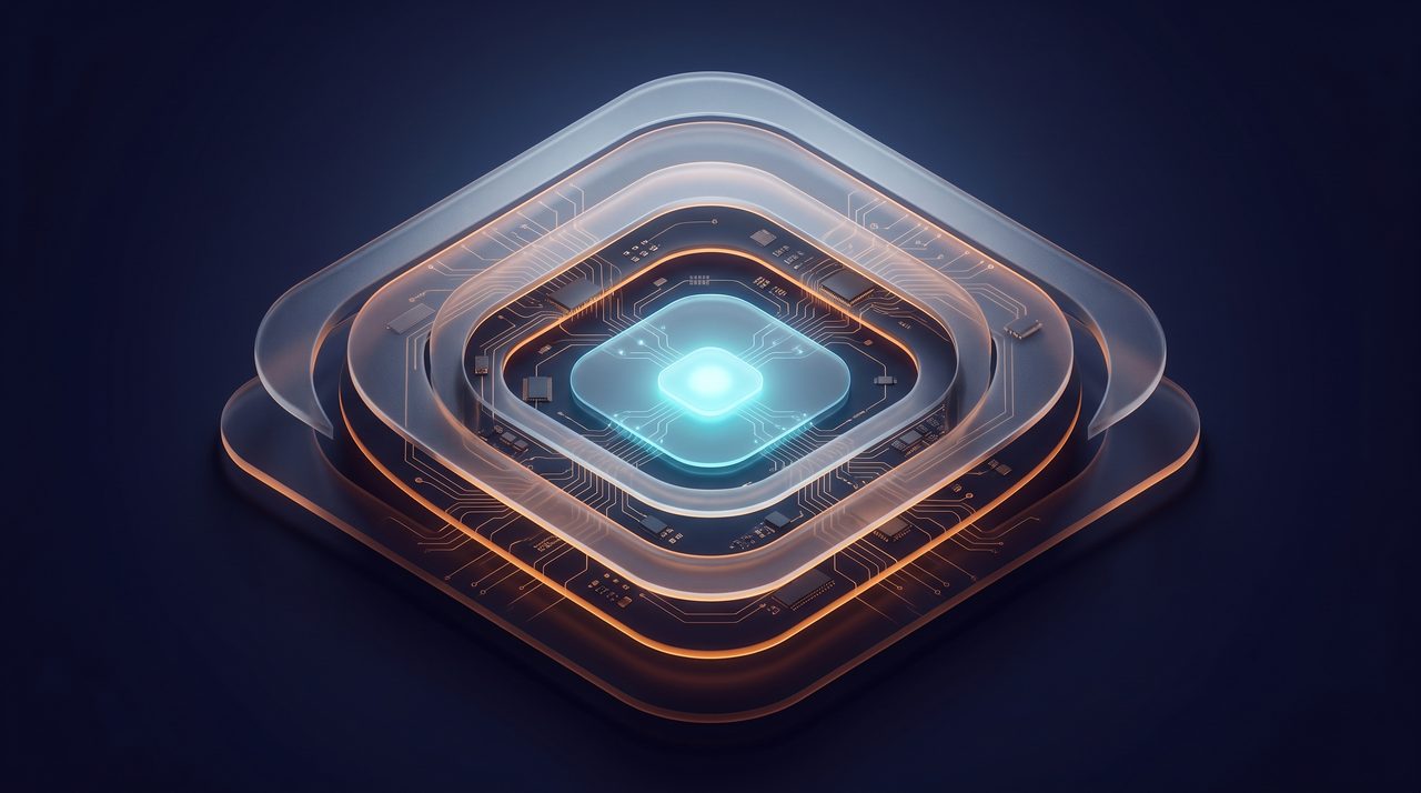
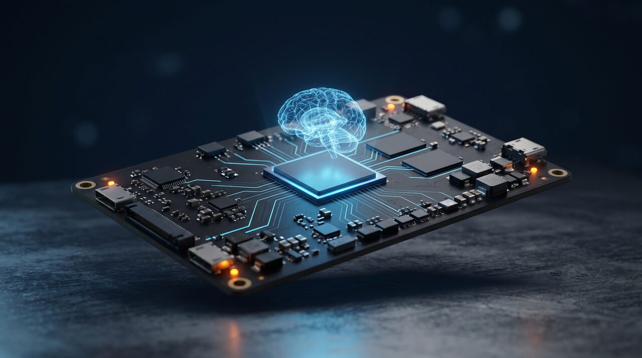
For the embedded Linux engineer, this split changes the job. The board is no longer a data-collection endpoint that forwards work upstream. It is where the work happens. That places more importance on the component that makes local inference possible: the accelerator.
AI accelerators: the silicon arms race
The hardware you choose determines much of what follows — the models you can run, the power budget you live within, and the software stack you will spend months integrating.
NPUs, TOPS, and the new performance tiers
The largest change of the past two years is that dedicated neural processing units (NPUs) have improved by roughly an order of magnitude and are now standard across the whole compute spectrum. A rough map of the landscape, from microcontroller NPUs to dev kits and across several vendors:
| Class | Representative silicon | AI performance |
|---|---|---|
| Microcontroller / TinyML | STMicroelectronics STM32N6 (Neural-ART) | ~0.6 TOPS INT8 (3 TOPS/W) |
| Integrated SoC NPU | NXP i.MX 8M Plus | ~2.3 TOPS |
| Integrated SoC NPU | Rockchip RK3588 | ~6 TOPS INT8 |
| Integrated SoC NPU | TI TDA4VM (Jacinto) | ~8 TOPS |
| Discrete accelerator | Google Coral Edge TPU | 4 TOPS INT8 (~2 W) |
| Discrete accelerator | Hailo-8 (M.2 module) | 26 TOPS INT8 |
| Laptop / phone NPU | Qualcomm Snapdragon X Elite | ~45 TOPS |
| Laptop / phone NPU | Intel Lunar Lake (Core Ultra 200V, NPU4) | up to 48 TOPS |
| Laptop / phone NPU | AMD Ryzen AI 300 | up to 50 TOPS |
| Robotics / vision module | NVIDIA Jetson Orin Nano Super | up to 67 TOPS |
| Robotics / vision module | NVIDIA Jetson Orin NX | up to 157 TOPS |
| Robotics / vision module | NVIDIA Jetson AGX Orin | up to 275 TOPS |
| High-end edge dev kit | NVIDIA Jetson AGX Thor | ~2070 FP4 TFLOPS (40–130 W) |
A caution about TOPS. Trillions of operations per second is a peak-throughput headline number, and it tells you little about real-world performance on your workload. The parts above also span different device classes — a microcontroller NPU, an integrated SoC NPU, a discrete accelerator module, and a full compute module — which are not measured the same way. The figure says nothing about the numeric precision assumed (INT8, INT4, or FP4), memory bandwidth, on-chip SRAM, thermal sustainability, or how well your model maps onto the accelerator’s execution units. A 275-TOPS module that is memory-starved on a vision-language model can perform worse than a lower-TOPS part with a better-balanced architecture. Use TOPS as a first-pass filter, then benchmark your actual model.
How edge accelerators achieve their efficiency
Understanding how NPUs achieve speed and efficiency is what lets you write software that uses them well. Three architectural techniques do most of the work:
- Systolic arrays for matrix multiplication — the dense linear algebra at the core of neural networks — arranged so data flows through a grid of multiply-accumulate units with little control overhead.
- Dedicated memory hierarchies designed to minimise data movement, because on modern silicon, moving data costs far more energy than the arithmetic. Keeping weights and activations close to the compute units is the main objective.
- Reduced-precision arithmetic — INT8 and increasingly INT4 — that keeps acceptable accuracy while cutting the compute and memory footprint.
The third point is where your work as an engineer meets the silicon. Quantization is no longer optional; it is a requirement for edge inference. A model trained in FP32 in the cloud must be quantized to INT8 or INT4 to run efficiently on an edge NPU, and doing that well — post-training quantization versus quantization-aware training, per-channel versus per-tensor scaling, handling outlier activations — is becoming a core embedded-AI skill. Heterogeneous SoC integration is delivering roughly 3 to 5 times better energy efficiency per inference operation with each generation (Research Intelo), and quantization is how you capture that efficiency.
The power spectrum: from sub-50 mW MCUs to 15 W NPUs
A useful way to think about the coming decade is that edge AI is not one thing. It is a spectrum that has widened at both ends. Vendors now embed ML accelerators across every processor tier — from Cortex-M class microcontrollers drawing under 50 mW for TinyML workloads, up to high-performance edge NPUs consuming as much as 15 W, and beyond that to the 130 W dev-kit class such as Jetson Thor.
Choosing the right point on that spectrum is the central design decision, and it is a familiar embedded trade-off in a new form:
- A battery-powered sensor node doing keyword spotting or anomaly detection wants the microcontroller end: milliwatts, TinyML, INT8 models measured in kilobytes.
- A smart camera or industrial gateway doing continuous computer vision wants a mid-tier NPU or a discrete accelerator in the single-digit-watt range.
- An autonomous robot or multi-camera vision-language system justifies a Jetson-class module and its power and thermal budget.
If this choice is wrong, software optimisation cannot recover it: an over-provisioned part drains the battery, and an under-provisioned one drops frames. The range of available parts is now wide enough that there is an accelerator tier for essentially every power envelope.
Where this leaves us
The foundation is in place. In 2026, edge AI has moved decisively from “collect data, send to cloud” toward “run the model where the data is.” The market forecasts, however they are scoped, point up. And the silicon — NPUs spanning sub-50 mW microcontrollers to 2000-plus-TFLOP dev kits — has matured to the point where the hardware is rarely the limiting factor.
That means the harder work moves up the stack. The open questions now are on the software side: how do you build, harden, and maintain the embedded Linux platform that turns this silicon into a deployable product, and how do you keep improving models across a fleet of devices without moving everyone’s private data back to a central server? Building that platform is the substance of our Embedded Linux and Yocto training.
Key takeaways
- Edge AI has changed the default from cloud inference to on-device inference, driven by latency, bandwidth and cost, reliability, and privacy regulation.
- Training stays largely in the cloud; inference increasingly runs on the device, which makes the accelerator the component that shapes the rest of the design.
- Accelerators now span from sub-1 TOPS microcontroller NPUs (STM32N6) through integrated SoC NPUs (i.MX 8M Plus, RK3588) and discrete modules (Coral, Hailo-8) to Jetson-class modules and dev kits. Choose by power envelope and workload, and treat TOPS as a first-pass filter only.
- Quantization to INT8 or INT4 is a required skill for edge inference, not an optional optimisation.
Further reading
- STL Partners — Edge AI market forecast and BCC Research — Global Edge AI Market.
- MarketsandMarkets — Edge AI Hardware Market and Mordor Intelligence — Edge AI Accelerators Market.
- Research Intelo — Edge AI Hardware (TinyML Processor) Market.
- Accelerator specifications: NVIDIA Jetson Thor, Hailo-8, and STMicroelectronics STM32N6.